FIB-SEM GAIA 3
General Information
Unit
CNR-ICCOMTechnique
Key Instrumentatiom
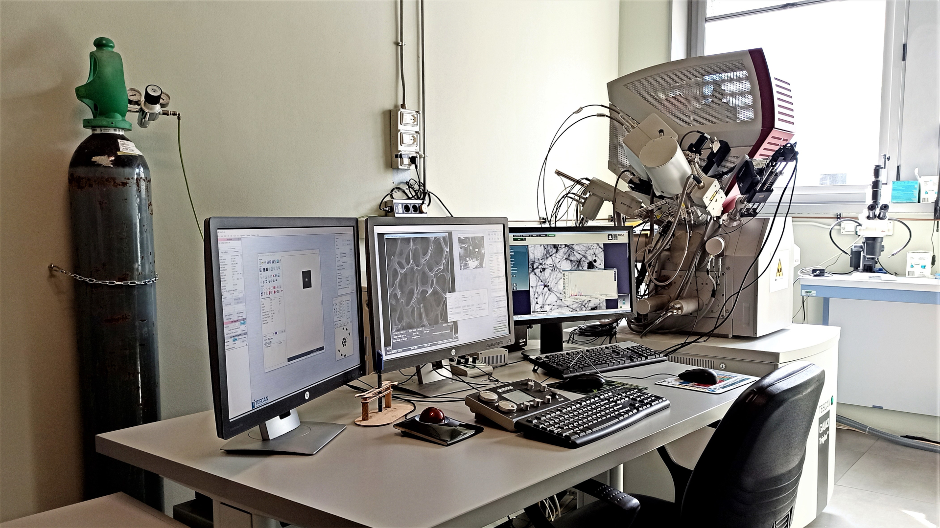
The Tescan GAIA 3 FIB‑SEM system at the CNR‑ICCOM unit is a high‑performance Dual Beam platform designed for advanced nanoengineering, microanalysis and high‑resolution imaging across a wide range of scientific and industrial applications. Its configuration ensures that the focal points of the electron beam and the gallium ion beam coincide, enabling simultaneous SEM imaging during FIB milling and providing exceptional precision, throughput and stability for all ion‑beam‑assisted operations. The instrument supports analytical workflows such as EDS microanalysis and high‑resolution SEM‑STEM imaging, allowing detailed characterization of materials, coatings, semiconductor structures, renewable‑energy devices, cultural‑heritage samples and agri‑food matrices. GAIA 3 is optimized for demanding nano‑fabrication tasks, including preparation of ultra‑thin TEM lamellae, delayering of multilayer devices, nanopatterning, site‑specific cross‑sectioning and high‑resolution 3D reconstructions. Its versatile operating modes—UH‑Resolution, Analysis and Depth—allow users to tailor imaging and milling conditions to the specific requirements of each sample. The system also supports electron‑beam lithography and precise ion‑beam surface processing for micro‑ and nano‑structuring. With industry‑leading EDS signal detection and outstanding STEM/TEM imaging capabilities, GAIA 3 provides a robust platform for metrological investigations, technology‑transfer activities and consultancy services requiring accurate structural, compositional and morphological analysis. This multifunctional instrument offers researchers and companies a powerful tool for comprehensive nanoscale characterization and fabrication.
Technical description
The Tescan GAIA 3 FIB‑SEM at the CNR‑ICCOM unit integrates a high‑resolution field‑emission SEM with a focused gallium ion beam, enabling advanced imaging, microanalysis and nanoscale material processing within a single platform. The SEM column is equipped with detectors for secondary and backscattered electrons, while the FIB column allows precise milling for site‑specific cross‑sections and preparation of high‑quality ultra‑thin TEM lamellae. Its unique three‑lens electron‑optical design provides dedicated modes for extreme high‑resolution imaging, enhanced depth of focus, distortion‑free ultra‑low‑magnification imaging and real‑time 3D stereo visualization. The smart chamber geometry enables simultaneous FIB milling and EBSD pattern acquisition without repositioning the sample, ensuring best‑in‑class accuracy for 3D‑EDS and crystallographic reconstructions.
GAIA 3 offers three optimized operating modes:
– UH‑Resolution mode, combining immersion optics with a crossover‑free beam for 1 nm resolution at 1 keV
– Analysis mode, using the Analytical lens for EDS, EBSD and simultaneous SEM imaging during FIB operations
– Depth mode, which couples the UH‑resolution lens with the IML lens to increase probe current while maintaining excellent resolution and large depth of focus.
This configuration makes GAIA 3 a powerful tool for materials science, semiconductor analysis and nanoscale engineering.Research areas and applications
-The TESCAN GAIA3 integrates a field emission SEM with a FIB
The SEM unit is equipped with detectors for secondary and backscattered
It allows preparation of high-quality ultra-thin TEM lamellae. It has a unique 3-lens electron optical design capable of dedicated modes for extreme high-resolution imaging, enhanced depth of focus, undistorted ultra-low magnification imaging, and live 3D stereo imaging. The smart chamber design of the instrument allows for the simultaneous milling and collection of EBSD patterns without the need to move the sample. This flexibility will provide best-in-class accuracy for 3D-EDS.
-GAIA3 is the ideal platform
UH-RESOLUTION mode: This mode is achieved by the unique combination of immersion optics and crossover-free mode for ultra-high resolution imaging at low energies. Avoiding any crossover in the column reduces the Boersch effect and further optimizes the electron beam to yield superior resolution of 1 nm at 1 keV.
ANALYSIS mode: This mode is implemented by means of the Analytical lens. It is well suited for analysis such as EDS and EBSD, as well as simultaneous SEM imaging during FIB operations such as cross-sectioning and FIB-SEM tomography.
DEPTH mode: The UH-resolution lens can be used in combination with the IML lens which allows for increasing the probe current while maintaining excellent resolution and enabling large depth of focus.Science highlights
Salvatore Impemba, Giacomo Provinciali, Jonathan Filippi, Cristina Salvatici, Enrico Berretti, Stefano Caporali, Martina Banchelli, Maria Caporali. International Journal of Hydrogen Energy (2024). https://doi.org/10.1016/j.ijhydene.2024.03.162
Walter Giurlani, Enrico Berretti, Alessandro Lavacchi, Massimo Innocenti. Analytica Chimica Acta. (2020). https://doi.org/10.1016/j.aca.2020.07.047
Samuele Fanetti; Sebastiano Romi; Enrico Berretti; Michael Hanfland; Emin Mijit; Frederico Alabarse; Philip Dalladay-Simpson; Federico Gorelli; Roberto Bini; Mario Santoro -The Journal of Chemical Physics (2023). https://doi.org/10.1063/5.0167748
Experimental team

- CNR-ICCOM
- Researcher