LabRAM Odyssey
General Information
Technique
Key Instrumentation
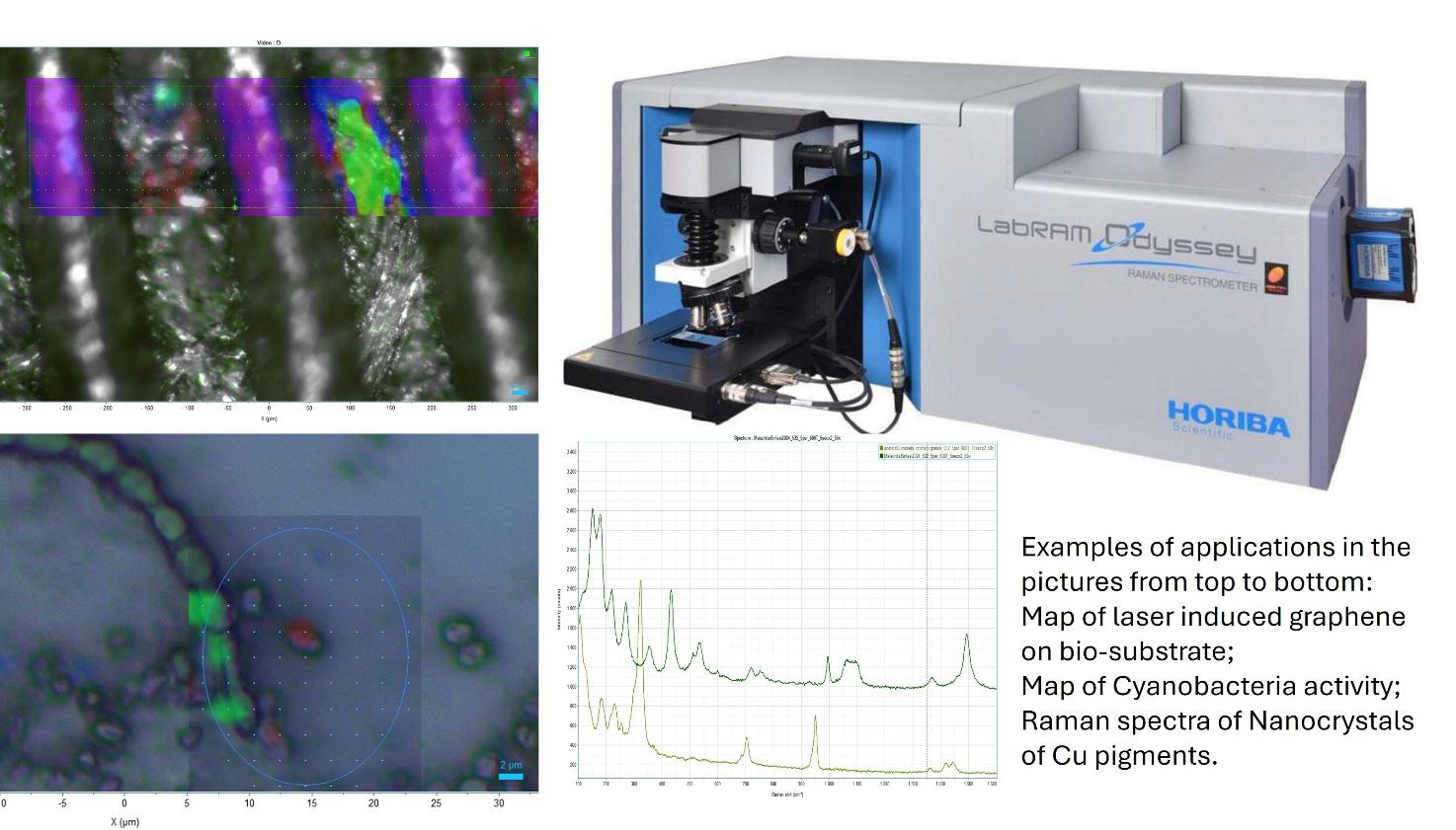
Raman Confocal MicroscopeRaman spectroscopy works by shining a laser onto a sample and analyzing the minute amount of scattered light that has shifted in energy (Raman scattering), providing a distinct chemical fingerprint for material characterization. Raman microscopy, which combines a Raman spectrometer with an optical microscope with a high magnification objective, is able to concentrate the laser beam on a sub-micron spot (about 1 µm or less) and at the same time to collect Raman signal; it can provide high-resolution information on a micro- and nano-meter scale, making it helpful in studying a material’s local composition, structure, and properties. Collecting Raman spectra at multiple points and constructing a spatially resolved map provides detailed insights into material properties such as composition, structure, defects, phase composition, interphase, etc. Raman imaging allows for non-destructive, high-resolution characterization of variations within a material sample. The LabRAM Odyssey Raman spectrometer offers advanced confocal imaging capabilities in both 2D and 3D, ideal for micro and macro measurements, high sensitivity, high spatial and spectral resolutions from Vis to NIR. The instrument offers high level of automation like a laser switch, an automated objective turret or an automated spatial calibration.
Technical description
Horiba LabRAM Odyssey, equipped with 800 mm single stage optimized spectrometer to achieve extremely high spectral resolution: better than 0.3 cm -1 with all laser source. Three holographic gratings at: 1800 gr/mm blazed at 500 nm (spectral range 325-900nm); 600 gr/mm holographic grating blazed at 500 nm (spectral range 360-1250nm); 300gr/mm ruled grating blazed at 1000nm (spectral range 600-4000nm). The spectrometer includes 3 lasers (532, 633, and 785 nm), motorized filter kit complete with EDGE interference filter for Stokes measurements starting from 50 cm -1 . Raman Confocal Microscopy, with motorized XYZ stage and spatial resolution of a 100 nm. Objectives 5x, 10x, 100x, 50xLWD (long working distance), possibility to investigate large sample.
Research areas and applications
Investigation of a wide range of materials, including polymers, ceramics, semiconductors, and nanomaterials. Able to investigate complex sample such as biological systems, cultural heritage, photovoltaic and fuel cell, composite, pharmaceutical products and so on. Key applications include: Chemical Identification, Structural Analysis, Defect and Purity Assessment, Stress and Strain Measurement, Phase Transitions. Mapping and Imaging: when combined with a microscope, it can generate high-resolution chemical images that show the distribution of different components or properties across a sample surface or within different layers.
Science highlights
R. R. Jones, D. C. Hooper, L. Zhang, D. Wolverson, and V. K. Valev,
Nanoscale Research Letters 14:231 (2019). https://doi.org/10.1186/s11671-019-3039-2S. Schlücker, Angewandte Chemie International Edition, 53(19), 4756–4795 (2014)
https://doi.org/10.1002/anie.201205748
Experimental team
- Silvia Orlanducci
- NAST Centre - University of Rome Tor Vergata

- Valeria Guglielmotti
- NAST Centre - University of Rome Tor Vergata

- Emanuela Tamburri
- NAST Centre - University of Rome Tor Vergata