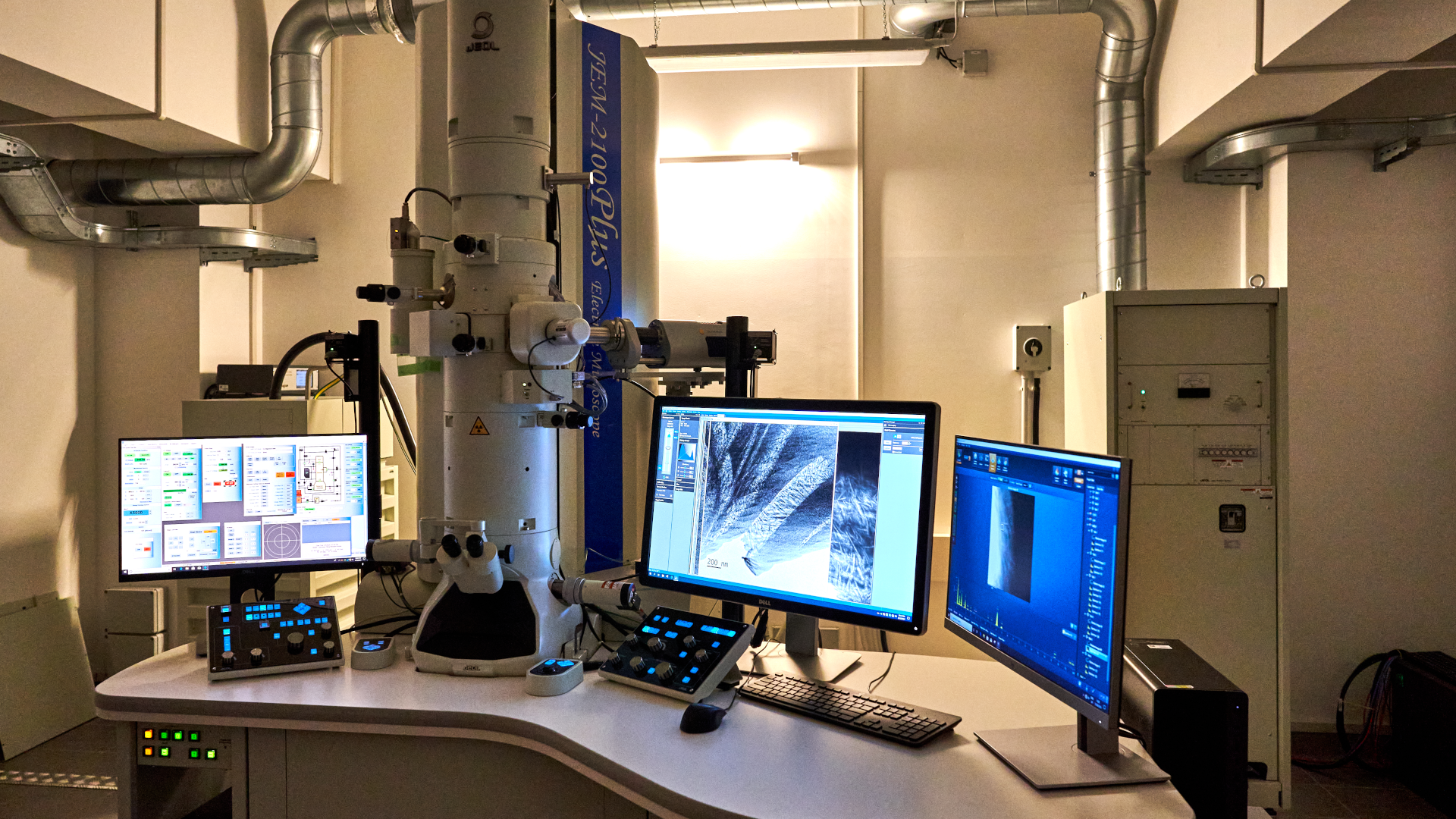
SEM ZEISS GEMINI
General Information
Technique
Key Instrumentation
Field Emission Scanning Electron Microscope, Zeiss Gemini 500The ZEISS Gemini SEM at the University of Milano‑Bicocca unit is a high‑performance field‑emission scanning electron microscope designed for advanced morphological, compositional, and crystallographic analysis of a wide range of materials. With a nominal resolution of 1.2 nm, the system enables high‑definition imaging of surface features, microstructures, and nanoscale details, making it suitable for research in materials science, nanotechnology, geology, and life sciences. The microscope integrates a complete micro‑analytical suite combining energy‑dispersive (EDS) and wavelength‑dispersive (WDS) X‑ray spectroscopy, allowing precise elemental identification, quantitative analysis, and high‑resolution chemical mapping. This dual‑detector configuration enhances sensitivity across the periodic table and supports the investigation of complex, multi‑phase systems. An EBSD detector is incorporated for crystallographic characterization of sample surfaces, enabling the determination of grain orientation, phase distribution, texture, and strain fields. This capability is essential for studies involving deformation mechanisms, thin‑film microstructure, and the correlation between crystallography and material properties. The Gemini electron‑optical column ensures stable beam performance at low accelerating voltages, facilitating high‑contrast imaging of beam‑sensitive or low‑Z materials. Automated stage control, advanced imaging software, and flexible detection modes support efficient workflows and multi‑modal data acquisition. Overall, the ZEISS Gemini SEM provides a powerful and versatile platform for researchers and industrial users requiring high‑resolution imaging, robust micro‑analysis, and detailed crystallographic insight.
Technical description
The ZEISS Gemini 500 SEM at the University of Milano‑Bicocca unit is a high‑performance field‑emission scanning electron microscope designed for advanced morphological, compositional, and crystallographic analysis. Operating between 1 and 30 kV, it provides a nominal resolution of 1.2 nm, enabling high‑definition imaging of surface features and nanoscale structures. In addition to standard in‑chamber SE and BSE detectors, the system includes in‑lens SE/BSE detectors that deliver enhanced contrast and high‑resolution imaging at low accelerating voltages. A STEM detector allows transmission‑mode observation of thin specimens and biological samples, expanding the analytical versatility of the instrument. The microscope is equipped with a Bruker integrated EDS/WDS micro‑analytical system optimized for light‑element detection, enabling precise elemental identification, quantitative analysis, and high‑resolution chemical mapping. Crystallographic characterization is supported by a Bruker EBSD detector, complemented by Argus FSE and BSE detectors for orientational contrast imaging and detailed grain‑structure analysis. This combination of detectors and analytical modules makes the Gemini 500 a powerful tool for sub‑micrometre‑scale investigations of solid materials, thin films, nanostructures, and biological tissues, supporting both academic research and industrial applications.
Research areas and applications
General mineralogy, advanced organic-inorganic hybrid functional nanomaterials, mineral forms for nuclear waste, dangerous airborne mineral dusts and fibers, REE and critical metals
Science highlights
Experimental team

- Giancarlo Capitani
- University of Milano Bicocca
- Professor