SEM ZEISS SIGMA
General Information
Unit
CSGITechnique
Key Instrumentation
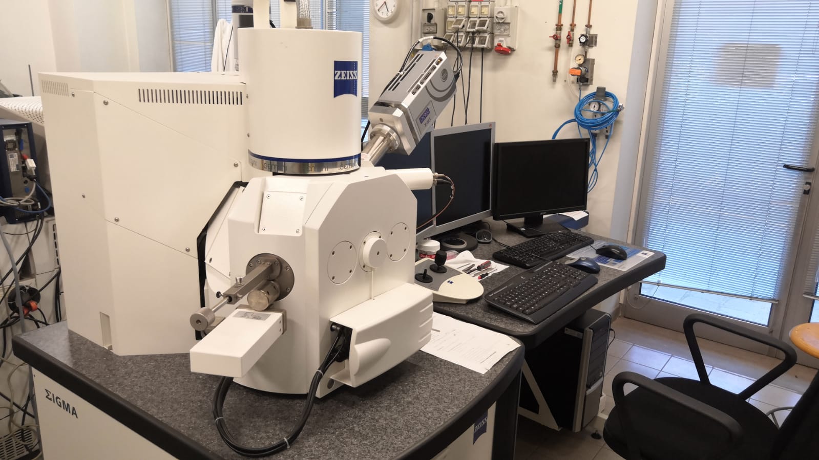
The SEM ZEISS Sigma at the CSGI – University of Florence unit is a high‑performance field‑emission scanning electron microscope designed for advanced morphological, compositional, and microstructural analysis of a wide range of materials. Its field‑emission source ensures a highly stable, bright electron beam, enabling high‑resolution imaging at both high and low accelerating voltages, which is essential for the investigation of nanostructured, beam‑sensitive, or low‑Z materials.
The system is equipped with multiple electron detectors, including secondary‑electron (SE) and backscattered‑electron (BSE) detectors, allowing detailed characterization of surface topography, compositional contrast, and crystallographic features. An integrated EDS detector provides elemental identification and quantitative microanalysis, supporting high‑resolution chemical mapping and enabling correlation between morphology and composition. The microscope’s variable‑pressure capabilities allow the examination of non‑conductive or environmentally sensitive samples without the need for conductive coatings, expanding its applicability to polymers, biological tissues, gels, and hydrated materials. The Gemini electron‑optical column ensures excellent imaging performance at low kV, delivering enhanced contrast and minimized charging effects. Automated stage control and intuitive imaging software support precise navigation, multi‑area acquisition, and efficient workflow management.
The system’s versatility makes it suitable for applications in materials science, nanotechnology, geology, cultural‑heritage studies, and life sciences. Overall, the ZEISS Sigma SEM provides a robust and flexible platform for researchers and industrial users requiring high‑resolution imaging, reliable microanalysis, and comprehensive characterization of complex materials.
Technical description
The ZEISS Sigma SEM at the CSGI – University of Florence unit is a high‑resolution field‑emission scanning electron microscope designed for advanced morphological and compositional analysis of a wide range of materials. Its GEMINI electron‑optical column provides a stable, bright beam and enables high‑contrast imaging at very low accelerating voltages, down to 100 V, making the system particularly suitable for non‑conductive samples or materials with poor electronic contrast that cannot be coated or chemically modified.
The instrument is equipped with an In‑Lens detector for high‑resolution surface imaging, complemented by conventional SE and BSE detectors for detailed topographic and compositional contrast.
An integrated Oxford Instruments EDS system supports elemental identification, quantitative microanalysis, and the acquisition of high‑resolution X‑ray emission maps, enabling precise correlation between morphology and chemical composition.
The variable‑pressure operating mode allows the examination of insulating, hydrated, or beam‑sensitive specimens without conductive coatings, expanding the applicability of the system to polymers, biological tissues, gels, and hybrid materials.
Automated stage control and advanced imaging software ensure accurate navigation, reproducible acquisition conditions, and efficient workflow management.Research areas and applications
Thanks to its flexibility, the Zeiss Sigma microscope finds many applications in the investigation of morphology and chemical composition of solids, also without metal coatings or chemical treatments. Materials Science (polymers, fibers, semiconductors, metals, alloys,…), life sciences (micro- and nanostructure of microrganisms, bones, prosthesis,…), geosciences and natural resources (rocks, minerals,…) and, more generally, industrial applications (such as in the case of powders) are some examples.
Science highlights
- Size and distribution of palladium nanoparticles electrodeposited on graphite, Saldan et al. https://doi.org/10.15407/fm25.01.082
- PVA-based peelable films loaded with tetraethylenepentamine for the removal of corrosion products from bronze, Guaragnone et al. https://doi.org/10.1016/j.apmt.2019.100549
- Modifying the crystallization of amorphous magnesium-calcium phosphate nanoparticles with proteins from Moringa oleifera seeds, Gelli et al. https://doi.org/10.1016/j.jcis.2021.01.008
