TEM JEOL
General Information
Technique
Key Instrumentation
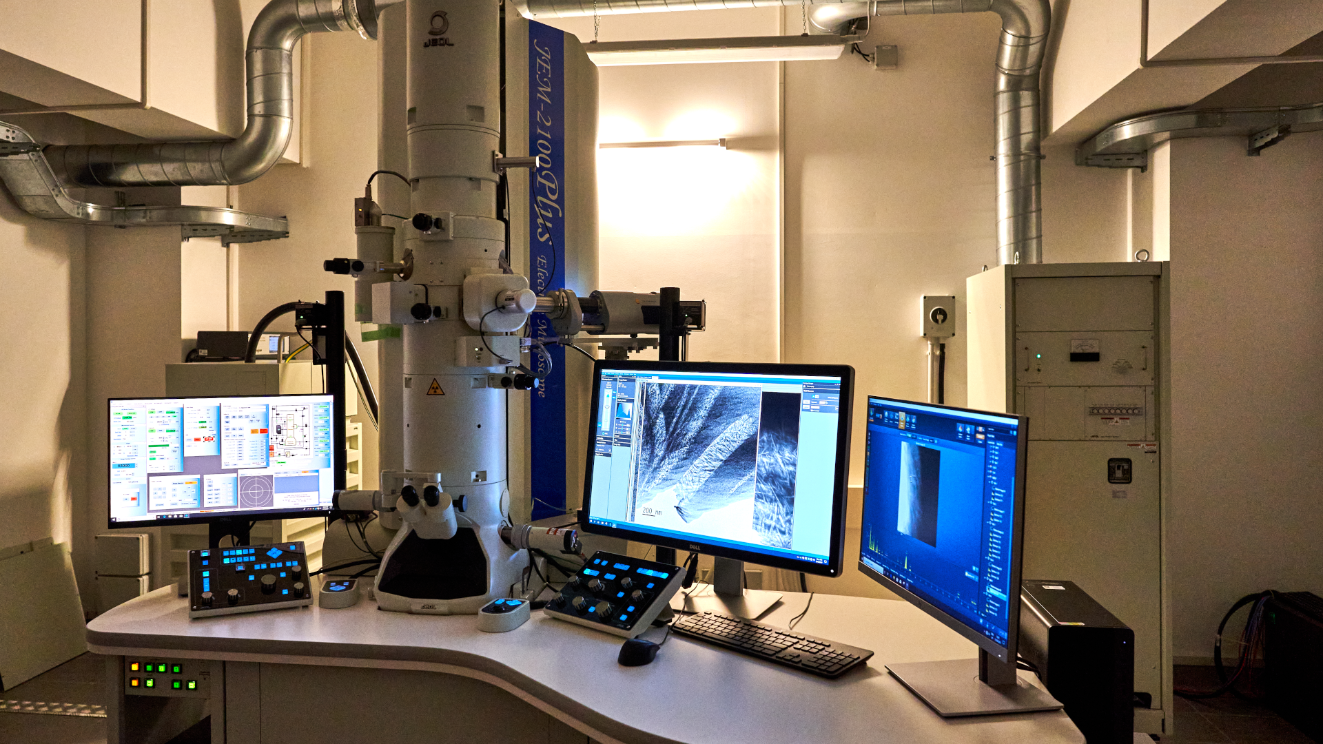
Transmission Electron Microscope - JEM 2100Plus with EDSThe TEM JEOL available at the University of Milano‑Bicocca unit is a versatile high‑resolution instrument designed for detailed morphological and structural characterization of inorganic, organic, polymeric, and biological materials. Equipped with a LaB₆ thermionic emitter, it operates across an accelerating‑voltage range of 80 to 200 kV, allowing users to optimize imaging conditions for both beam‑sensitive samples and more robust crystalline materials. The microscope provides a point‑to‑point resolution of 0.24 nm, enabling the visualization of lattice fringes, nanoscale interfaces, and fine structural details in bright‑field and diffraction modes. Its imaging system includes a high‑sensitivity 9‑megapixel CMOS camera that supports rapid acquisition of high‑contrast micrographs and electron‑diffraction patterns, facilitating both qualitative inspection and quantitative structural analysis. The integrated EDS micro‑analysis system allows precise elemental identification and mapping, enabling correlation between chemical composition and microstructural features at the nanometer scale. The instrument supports a wide magnification range suitable for multi‑scale investigations, from general morphological surveys to high‑resolution studies of nanostructures, thin films, and biological assemblies. Stable stage control ensures accurate positioning and tilt capabilities for crystallographic analysis and orientation studies. Overall, the TEM JEOL provides a robust and flexible platform for researchers and industrial partners requiring high‑quality imaging, reliable micro‑analysis, and comprehensive nanoscale characterization across diverse classes of materials.
Technical description
The JEOL JEM‑2100 Plus TEM at the University of Milano‑Bicocca unit is a high‑performance transmission electron microscope designed for advanced structural and analytical characterization of inorganic, organic, and biological materials. Equipped with a LaB₆ emitter, it operates between 80 and 200 kV, allowing users to optimize imaging conditions for both beam‑sensitive and highly crystalline samples. The high‑resolution objective pole piece provides a point‑to‑point resolution of 0.24 nm in TEM mode, enabling the visualization of lattice fringes, nanoscale interfaces, and fine structural details. The instrument also supports STEM operation, acquiring BF and HAADF images with a nominal resolution of 1 nm, ideal for Z‑contrast analysis and nanoscale compositional studies. An 80 mm² Oxford EDS detector enables spot analysis and chemical mapping, ensuring precise elemental identification and correlation with structural features. Image acquisition is performed using a 9‑megapixel Gatan CMOS camera, offering high sensitivity and rapid capture of micrographs and diffraction patterns. A dedicated in‑gap aperture reduces beam damage on sensitive materials, including biological specimens. The wide tilt range (±45° with a standard double‑tilt holder), combined with the instrument’s high‑resolution capabilities and versatile detection modes, makes the JEM‑2100 Plus a powerful platform for comprehensive nanoscale investigations across diverse material classes.
Research areas and applications
nanoparticles, semiconductors, hazardous mineral particles and fibres, proteins, citotoxicity studies, cell ultrastructure, nanoplastics
Science highlights
Experimental team

- Giancarlo Capitani
- University of Milano Bicocca
- Professor

- Melissa Saibene
- University of Milano Bicocca
- PostDoc