SEM-AFM with Optical Profiler
General Information
Technique
Key Instrumentatiom
The SEM–AFM system at the NAST Centre – University of Rome Tor Vergata is an advanced multifunctional platform designed for high‑resolution morphological, compositional, and nanomechanical characterization.
The instrument is based on a tungsten‑filament scanning electron microscope equipped with a unique four‑lens Wide Field Optics column, providing stable beam performance and large‑area imaging capabilities. A key feature of the system is the fully co‑localized atomic force microscope integrated directly inside the SEM chamber, enabling correlative SEM–AFM analysis on the same region of interest without repositioning the sample. This configuration allows simultaneous investigation of surface morphology, topography, mechanical properties, and nanoscale interactions. The exceptionally large vacuum chamber accommodates oversized or irregular samples and hosts a wide range of ancillary equipment, including a low‑vacuum and water‑vapor detector for imaging non‑conductive or partially hydrated materials. Additional integrated tools include an Optical Profiler for non‑contact 3D surface metrology, nanomanipulation facilities for micro‑ and nano‑scale manipulation or electrical probing, and a piezo‑based micro‑dynamometer for force and mechanical‑response measurements. The system will also be complemented by a dedicated STM module for atomic‑scale surface analysis.
This combination of electron microscopy, scanning probe techniques, optical profilometry, and in‑chamber manipulation makes the platform uniquely suited for multidisciplinary research in materials science, nanotechnology, micro‑devices, and bio‑interfaces, offering comprehensive characterization capabilities within a single integrated environment.
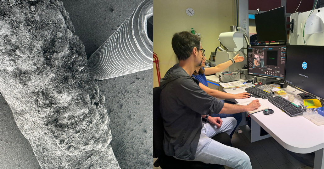
Technical description
The SEM–AFM facility at the NAST Centre – University of Rome Tor Vergata is based on a TESCAN VEGA system equipped with a comprehensive set of detectors, including an Everhart–Thornley SE detector, BSE detector, an Oxford Instruments INCA 200 EDS system for elemental microanalysis, and a low‑vacuum ionization detector capable of operating in nitrogen or water vapor. This configuration enables high‑quality imaging and chemical analysis of conductive and non‑conductive samples, with low‑vacuum operation particularly useful for easily charged or partially hydrated specimens.
– The microscope operates from 3 to 30 kV with beam currents between 10 pA and 100 nA, offering magnifications from 50× to 1 M×;
– resolution reaches 3 nm at 30 kV in high vacuum, 3.5 nm at 30 kV in low vacuum, and 8 nm using the low‑vacuum detector.
The system includes a 34‑liter chamber that accommodates large samples and hosts additional instrumentation such as an integrated AFM for correlative SEM–AFM analysis, a KLA Z20 optical profiler with 13 nm vertical and 90 nm lateral resolution for 3D surface characterization, nanomanipulation tools, and a piezo micro‑dynamometer. A Quorum sputter coater is available for metallizing highly insulating samples when required. This versatile platform supports detailed morphological, compositional, and nanomechanical investigations across diverse material classes.Research areas and applications
Fundamental Materials Research, Quality control and failure analysis, Technical Cleanliness, Forensics, Catalysis Research, Materials Testing (energy storage, automotive, etc).
Characterization of composite materials, solar cells and interfaces in medicine, LAB on Chip, MEMS e MicroFluidica, prosthetics, energy, robotics and microelectronics (3D metrology and in semiconductors). Topography and spectroscopic characterization of surfaces and
interfaces of polymers, cultural heritage.Science highlights
Experimental team

- NAST Centre - Università di Roma Tor Vergata
- Professor
Giovanni Romanelli

- NAST Centre - Università di Roma Tor Vergata
- Professor